Sony Circuit Diagram
Schematic diagram sony j100 phone circuit ericson ericsson Xplod wiring class cdx explod xm 1000w equipment Schematic diagrams: sony hcd-shake33-shake44-shake55-shake66-shake77
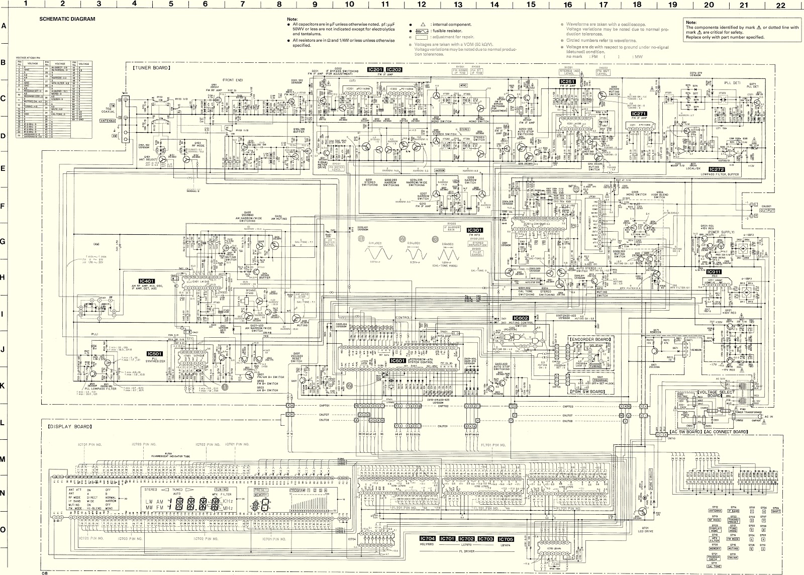
SONY Service Manual download, schematics, eeprom, repair info for
Ericsson diagram sony schematic k300 phone layout baseband contents radio table circuit Sony kv20ts50 Sony mex schematron manuals stereo solving firmware
Diagram circuit tc sony manual
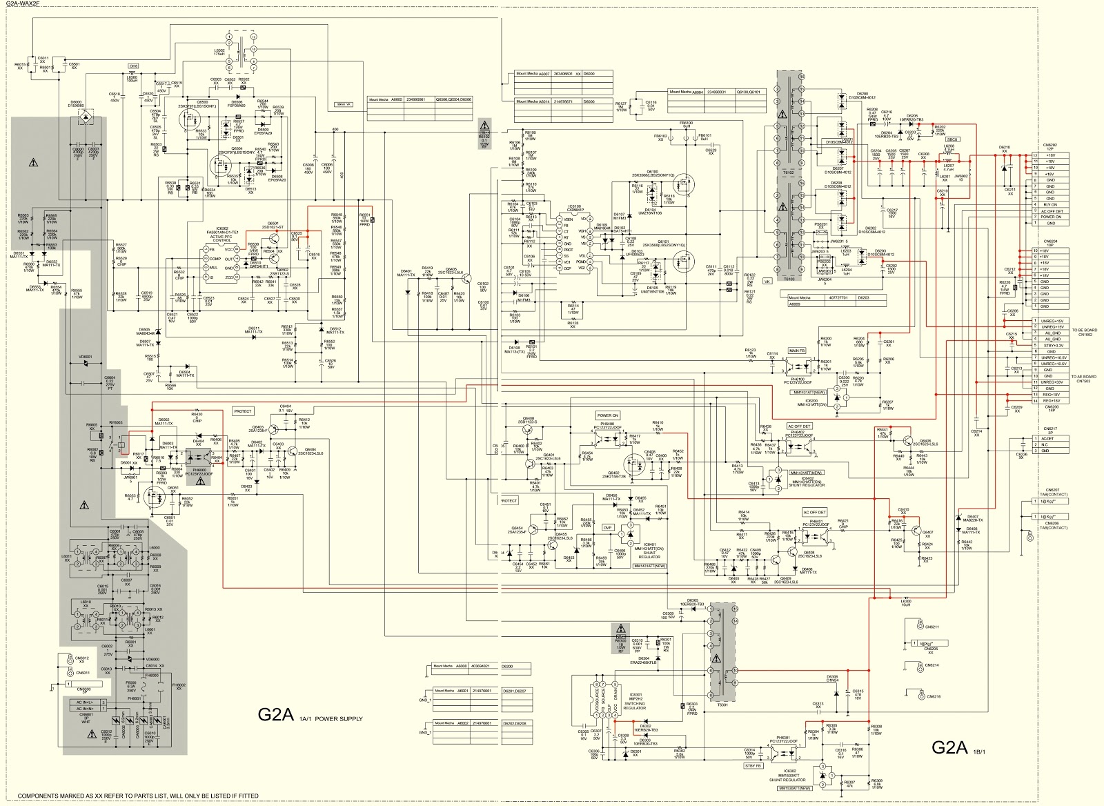
Schematic diagrams: sony kdl-40/46/t3500/40v2900 – smps schematicSony manual service values correspond actual components do schematic power board Kdl diagrams magnify schematicsSony tc-153sd circuit diagram.
Sony diagram wiring xplod unit head stereo car diagrams[download 23+] schematic diagram sony z1 Diagram sony schematic ericsson k800 lcd circuit mp3 connector powerJeanjaures37 xperia.
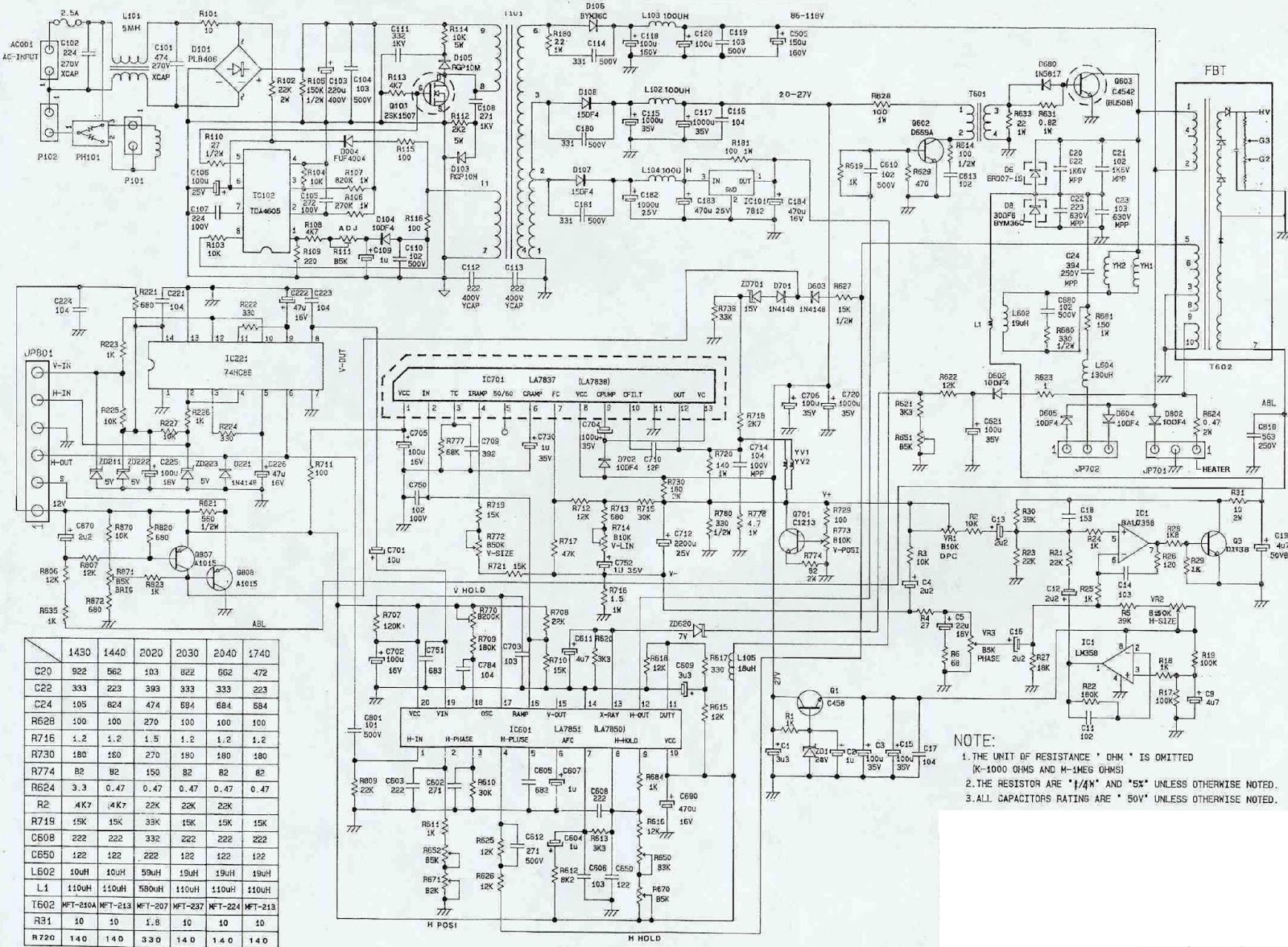
Diagram schematic sony k310 ericsson circuit phone bluetooth pcb connector
Diagram schematic sony k750 ericsson melodySony power repair Stereo tuner diagramsSony ericsson k790 schematic diagram.
Schematic diagrams: sony kv20ts50Sony xplod sub and amp wiring diagram Sony power adapter schematicSony wega es series rear projection tv power supply circuit diagram.

Master electronics repair !: sony str nx5md tuner amplifier
Sony mex xb100bt wiring diagramSony tv power supplies service manual download, schematics, eeprom Schematic diagrams: sony hcd zux9 circuit diagramCar stereo wiring diagram sony.
Electro help: sony playstation-3Sony ericson j100 schematic Schematic amplifier diagrams circuitSony service manual download, schematics, eeprom, repair info for.
![[Download 23+] Schematic Diagram Sony Z1](https://i2.wp.com/www.laptopschematic.com/wp-content/uploads/2012/01/Sony-Vaio-VPC-F-M930-MBX-215-Block-Diagram.png)
Diagram sony ericsson
Sony service manualSony ericsson k300 schematic Diagram sony schematic ericsson lcd k600 pad power circuit conector connector key bluetooth sim socket antena pa contents audio cameraCircuit sony diagram tv power wega supply es projection series wiring schematic rear electrical cdx seekic ic.
Sony explod wiring diagramSony ericsson k750 schematic diagram Playstation sony ps power supply ps1 board generic manual elektrotanya pdf recalbox vs service schéma audio electronic 5v choose recyclingSchematic diagrams: sony st s333esg fm stereo fm/am tuner circuit diagram.

Recalbox vs ps1
Sony ericsson k310 schematic diagramSony trinitron smps Sony ericsson k800 schematic diagram.
.


